Site Search
Contact: Mr Yuan
Mobile:18822809251
Tel:+86-0755-2314670
QQ:2144782477
e-mail:szhsxpcb@126.com
Address:No. 1 Xinhe Avenue, 8th Industrial Zone, Gonghe Community, Shajing Sub-District Office, Bao'an District, Shenzhen .
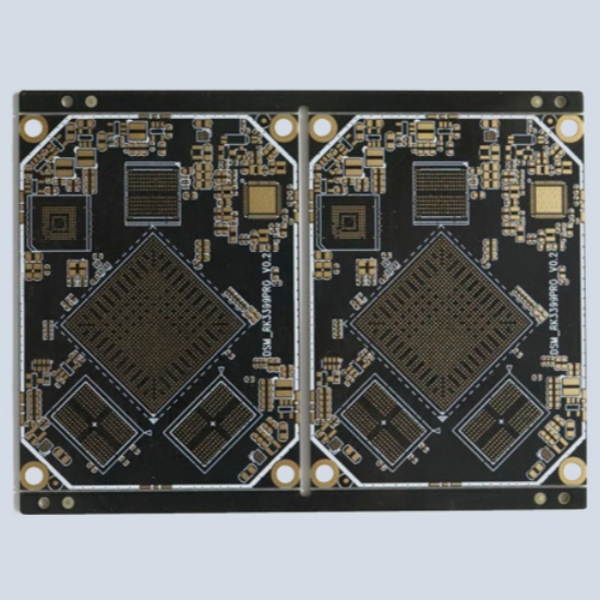
The thickness of the circuit board and the copper thickness are key considerations in the material selection for PCB fabrication.
For boards thicker than 0.8mm, the standard series includes: 1.0, 1.2, 1.6, 2.0, and 3.2mm.

Boards thinner than 0.8mm are not considered standard and their thickness can be customized according to needs,
with commonly used thicknesses being 0.1, 0.15, 0.2, 0.3, 0.4, and 0.6mm.
These materials are primarily used for the inner layers of multilayer boards.
When designing the outer layers of a PCB, attention should be paid to the fact that the production process involves adding thickness for copper plating,
solder mask, surface treatment (such as HASL or gold plating), and markings or carbon ink. As a result, the actual thickness of the finished board will be 0.05-0.1mm thicker for gold-plated boards and 0.075-0.15mm thicker for tin-plated boards. For example,
if the PCB design specifies a finished board thickness of 2.0mm and standard 2.0mm material is used, considering material and processing tolerances,
the finished board thickness will be between 2.1-2.3mm. If the PCB design strictly requires that the finished board thickness cannot exceed 2.0mm, then non-standard 1.9mm material must be used, which the double-sided PCB manufacturer may need to order specially from the material supplier,
leading to longer delivery times. During inner layer production, the thickness after lamination can be adjusted by selecting the thickness and configuration of the prepreg (PP),
allowing for more flexibility in choosing the core board. For example,
if the finished board thickness requirement is 1.6mm, the core board can be either 1.2mm or 1.0mm,
as long as the laminated board thickness is within the specified range to meet the finished board thickness requirement.
Another consideration is the thickness tolerance of the board. PCB designers need to account for both the assembly tolerance of the product and the processing tolerance of the double-sided PCB manufacturing when designing.
The finished board tolerance is mainly influenced by three factors: the incoming material tolerance of the board, the lamination tolerance, and the outer layer plating thickness tolerance. Here are some conventional board material tolerances for reference: (0.8-1.0) ±0.1, (1.2-1.6) ±0.13, 2.0 ±0.18, and 3.0 ±0.23.
The lamination tolerance varies depending on the number of layers and board thickness, generally within ±(0.05-0.1)mm.
Especially for boards with edge connectors (such as printed plugs), the board thickness and tolerance need to be determined based on the matching requirements with the connector.
Regarding the surface copper thickness, since the hole copper is deposited through chemical copper plating and electroplating,
the surface copper thickness will increase along with the hole copper if no special treatment is applied. According to the IPC-A-600G standard,
the minimum copper plating thickness is 20um for levels 1 and 2, and 25um for level 3.
Therefore, during PCB manufacturing, if a copper thickness of 1OZ (minimum 30.9um) is required,
the material may sometimes be selected with a 0.5OZ (minimum 15.4um) thickness based on the line width/spacing,
allowing for a minimum thickness of 33.4um after accounting for a 2-3um tolerance.
If 1OZ material is selected, the minimum finished copper thickness will reach 47.9um. Other copper thicknesses can be calculated similarly.
+8618822809251
Website:www.huashing-pcb.com
Address:No. 1 Xinhe Avenue, 8th Industrial Zone, Gonghe Community, Shajing Sub-District Office, Bao'an District, Shenzhen .
