Site Search
Contact: Mr Yuan
Mobile:18822809251
Tel:+86-0755-2314670
QQ:2144782477
e-mail:szhsxpcb@126.com
Address:No. 1 Xinhe Avenue, 8th Industrial Zone, Gonghe Community, Shajing Sub-District Office, Bao'an District, Shenzhen .
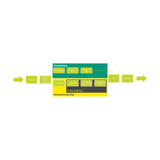
In the complex production of printed circuit boards, there are two typical manufacturing processes for the core processes of through-hole plating and structuring. A distinction is made between "pattern plating" and "panel plating". Depending on the requirements, layer structure and layout, KSG decides on the most suitable manufacturing process. A combination of both processes can also be used. ("semi-pattern plating") can be used. Design rules for this can be found at → 8.6 Design Rules | Outer layers/metallized layer.
General: Integration into the production process

+8618822809251
Website:www.huashing-pcb.com
Address:No. 1 Xinhe Avenue, 8th Industrial Zone, Gonghe Community, Shajing Sub-District Office, Bao'an District, Shenzhen .
