Site Search
Contact: Mr Yuan
Mobile:18822809251
Tel:+86-0755-2314670
QQ:2144782477
e-mail:szhsxpcb@126.com
Address:No. 1 Xinhe Avenue, 8th Industrial Zone, Gonghe Community, Shajing Sub-District Office, Bao'an District, Shenzhen .
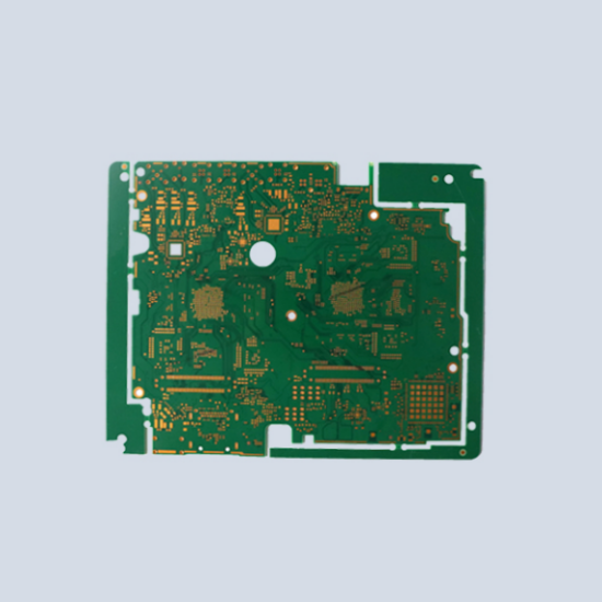
What are the common laminated structures of HDI multilayer boards?
The laminated structure is an important factor affecting the EMC performance of PCB board,
and is also an important means to suppress electromagnetic interference. With the emergence of high-speed circuits, the complexity of PCBs is also increasing. In order to avoid interference with electrical factors,
the signal layer and the power layer must be separated, so it involves the design of HDI multilayer panels.
So, what are the common laminated structures of HDI multilayer boards?

1. Simple one layered printing plate.
There are six layers of plate at one time, and the layering structure is (1 + 4 + 1).
This type of plate is the simplest, i.e. there are no buried holes in the internal multi-layer plate and it is completed with a single pressing.
Unlike multi-layered plates, there are several processes that need to be followed by laser drilled blind holes, among others.
2, the conventional one layer of HDI printed board
The laminated HDI6 laminate has a laminated structure of (1 + 4 + 1).
The structure of this type of plate is (1 + N + 1), (N ≥ 2, N coefficient), and this structure is currently the mainstream design of primary layered plate in the industry, with multiple layers with buried holes and needing secondary piezoation.
3, the conventional secondary layer of HDI printed board
The laminated structure of the secondary laminated HDI 8-layer board is (1 + + 1 + 4 + 1 + 1).
The structure of this type of plate is (1 + 1 + N + 1 + 1), (N≥ 2, N is an odd number),
and this structure is currently the mainstream design of secondary additive layers in the industry,
with multiple layers of plate with buried holes and needs to be crushed three times.
4, the second conventional secondary layer HDI printed board
The structure of the secondary laminated HDI 8 laminate is (1 + 1 + 4 + 1 + 1).
Structure of such plates (1 + 1 + N + 1 + 1), (N ≥ 2, N even),Although it is the structure of a secondary additive plate,
because the burial hole is not between (3-6) layers but between (2-7) layers,
this design can reduce the pressing once, so that the secondary additively HDI plate needs 3 pressing processes, and is optimized to 2 pressing procedures.
5. HDI for the secondary layer of blind hole stack design
The blind hole is stacked above the buried hole (2-7) layer,
and the second layer HDI8 layer board is stacked in structure (1 + 1 + 4 + 1 + 1).
The structure of this type of plate is (1 + 1 + N + 1 + 1), (N ≥ 2, N even), and the inner multilayer plate has buried holes and needs to be pressed twice.
6. HDI for the secondary layer of cross-layer blind hole design
The structure of the secondary laminated HDI 8 laminate is (1 + 1 + 4 + 1 + 1).
The structure of this type of plate is (1 + 1 + N + 1 + 1), (N ≥ 2, N is an odd number),
and this structure is a secondary layer plate that is difficult to make in the industry at present,
with multiple layers of plate buried in (3-6) layers, and it needs to be pressed three times.
7. Optimization of HDI plates with other laminated structures
Three layers of printed boards or more than three layers of PCB boards, can also be optimized, the complete three layers of HDI board, need 4 times lamination.
+8618822809251
Website:www.huashing-pcb.com
Address:No. 1 Xinhe Avenue, 8th Industrial Zone, Gonghe Community, Shajing Sub-District Office, Bao'an District, Shenzhen .
