Site Search
Contact: Mr Yuan
Mobile:18822809251
Tel:+86-0755-2314670
QQ:2144782477
e-mail:szhsxpcb@126.com
Address:No. 1 Xinhe Avenue, 8th Industrial Zone, Gonghe Community, Shajing Sub-District Office, Bao'an District, Shenzhen .
At higher frequencies, the signal degrades due to insertion loss. This can occur due to conflicting dielectric properties, copper profile, and surface finish.
Choose a low-tooth copper profile to avoid skin effects in your microwave and radio frequency circuits.
Pick ENIG, immersion tin, or ENEPIG surface finish to prevent signal losses.
Select a substrate with a low dielectric constant, low loss tangent, and stable electrical properties over a wide frequency range. Low Dk materials are usually PTFE-based, like Rogers RO4000 series or FR-4 with enhanced RF properties.
Before choosing the substrate, check their availability with your RF and microwave PCB manufacturer.
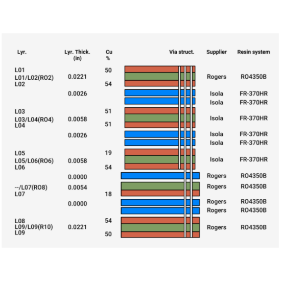
A hybrid stack-up with mixed materials is also a viable option for RF/microwave designs. Here, go for low Dk laminates specifically for layers with critical traces and FR-4 for the rest. This provides better layer customization for signal integrity, thermal management, and signal isolation.
Note that the chosen materials in hybrid stack-ups must have matching CTEs to avoid cracks during the lamination process.
At Sierra Circuits, we control curing parameters like temperature, pressure, and time to minimize inherent and residual stress, thus eliminating the risk of layer misalignment and delamination.

+8618822809251
Website:www.huashing-pcb.com
Address:No. 1 Xinhe Avenue, 8th Industrial Zone, Gonghe Community, Shajing Sub-District Office, Bao'an District, Shenzhen .
