Site Search


Product Name:
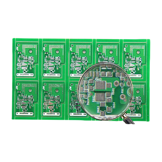
HDI First Order 8 Layers Tin Spraying

Product Code:
HDIPCB08001
HDI (First Order) 8-layer tin spray PCB features include:
1. High Density Wiring
The first order HDI design allows for high density circuit connections in a limited space for small and complex electronics.
2. Blind and Buried Vias Technology
HDI designs often employ blind and buried vias, which facilitate efficient signal connections between different layers, thereby reducing surface wiring complexity and improving circuit reliability.
3. Tin Spray Surface Treatment
Tin spraying as a surface treatment process provides good solderability and is suitable for the soldering requirements of most electronic components. The tin spray layer usually has good oxidation resistance and is relatively low cost.
4. Multi-layer structure
The 8-layer multilayer design provides space for proper layout of signal, ground and power layers, which can effectively reduce electromagnetic interference (EMI) and improve signal integrity.
5. Flexible Electronic Component Layout
HDI technology allows flexible layout of electronic components of various specifications and sizes, supporting the design needs of various modern electronic products.
6. Signal Integrity
With HDI's cabling design, the length of the signal transmission path can be significantly reduced, resulting in improved signal integrity and reduced latency, making it particularly suitable for high-speed signal transmission.
7. Thermal Management Performance
Multi-layer design and proper layout can help improve thermal performance, such as introducing ground layers in the power supply layer to disperse heat.
8. Wide range of applications
HDI first-order 8-layer tin-sprayed PCBs are widely used in smartphones, tablets, communication devices, medical devices, and other high-performance electronic products.
9. Increased Productivity
HDI's high-density design combined with the tin spray process can improve production efficiency and yield, suitable for large-scale production.
+8618822809251
Website:www.huashing-pcb.com
Address:No. 1 Xinhe Avenue, 8th Industrial Zone, Gonghe Community, Shajing Sub-District Office, Bao'an District, Shenzhen .
