Site Search
Contact: Mr Yuan
Mobile:18822809251
Tel:+86-0755-2314670
QQ:2144782477
e-mail:szhsxpcb@126.com
Address:No. 1 Xinhe Avenue, 8th Industrial Zone, Gonghe Community, Shajing Sub-District Office, Bao'an District, Shenzhen .
What knowledge is required for routing multi-layer PCBs?
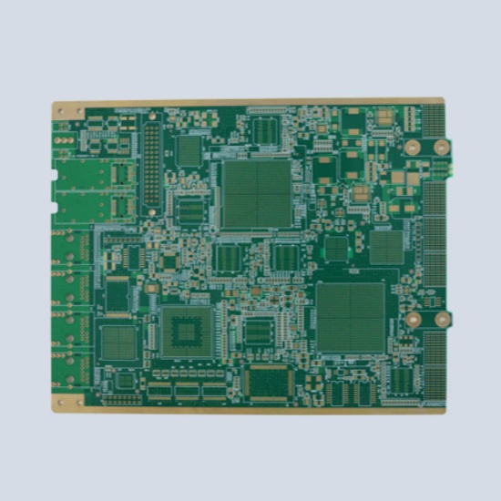
PCB routing is the process of laying out printed wires based on the PCB schematic diagram, wire list, and the required wire width and spacing. So, what knowledge is essential for routing multi-layer PCBs?

Routing should be as simple as possible while meeting the requirements. The preferred order for routing methods is single-layer, double-layer, and then multi-layer.
Ground wires should be placed alongside the input wires of analog circuits for shielding. Wires on the same layer should be evenly distributed, and the conductive area on each layer should be relatively balanced.
When changing the direction of signal wires, use diagonal or smooth transitions to avoid electric field concentration, signal reflection, and additional impedance.
Digital and analog circuits should be separated in routing to avoid mutual interference. Ground wires should be placed between signal lines of different frequencies to prevent crosstalk. Necessary breakpoints and test points should be designed for easy testing.
When grounding or connecting circuit components to the power supply, the wires should be as short and close as possible to reduce internal resistance.
Wires on upper and lower layers should be perpendicular to each other to reduce coupling. Avoid aligning or paralleling wires on upper and lower layers.
Multiple I/O lines of high-speed circuits, as well as I/O lines of differential amplifiers, balanced amplifiers, and other circuits, should be of equal length to avoid unnecessary delays or phase shifts.
When connecting PCB pads to large conductive areas, use thin wires with a length of no less than 0.5m for thermal isolation. The width of the thin wires should be no less than 0.13mm.
The wires closest to the edge of the SMB (Surface Mount Board) should be at a distance greater than 5mm from the edge. If necessary, ground wires can be placed closer to the edge of the SMB.
Common power and ground wires on double-sided SMBs should be placed near the edge of the SMB and distributed on both sides. For multi-layer SMBs, power and ground planes can be set up in the inner layers, connected to the power and ground wires on each layer through metallized holes. Large conductive areas, power lines, and ground lines in the inner layers should be designed as a mesh.
+8618822809251
Website:www.huashing-pcb.com
Address:No. 1 Xinhe Avenue, 8th Industrial Zone, Gonghe Community, Shajing Sub-District Office, Bao'an District, Shenzhen .
